The Microprocessor
Computer Science Homework Help
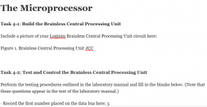
Task 4-1: Build the Brainless Central Processing Unit
Include a picture of your Logisim Brainless Central Processing Unit circuit here:
Figure 1. Brainless Central Processing Unit JCC
Task 4-2: Test and Control the Brainless Central Processing Unit
Perform the testing procedures outlined in the laboratory manual and fill in the blanks below. (Note that these questions appear in the text of the laboratory manual.)
· Record the first number placed on the data bus here: 5
· What do the following three switches need to be set to in order to perform the pass-through operation? /~A_Only = 0 /~Invert= 1 Logic/~Arith= 0
· Enter the second number you entered into the data bus here: 2
· What do the following three switches need to be set to in order to perform the ADD operation? /~A_Only = 1 /~Invert= 1 Logic/~Arith= 0
· Write down the number that appears in the accumulator here: 7
Describe other numerical additions and other operations you checked in order to verify your brainless CPU here: I repeated the additions several times using 3, 4 and 1 and toggled through several times till I got the correct addition.
After you are convinced your circuit is working properly, remove the 4-bit binary keyboard and set the ACC to Data Bus pin to 1. Did the output of the accumulator appear on the data bus? Yes.
How does the output of the ALU change? It changed to Hex E.
If the 4-bit binary keyboard was not removed and the ACC to Data Bus switch is set to 1, what would you expect to see displayed in the hex digit display attached to the data bus?
I expect to see whatever is supplied to the data bus in hex display.
Add the 4-bit binary keyboard back into your circuit and observe the hex digit display on the data bus for various keyboard values. Is the value on the hex digit display what you expected? Yes.
Explain Only 1 signal is being allowed to enter the buffer at a time. Therefore, the buffer is receiving only the output of the register.
Why do you think the register at the output of the ALU is called the ‘accumulator’? Because it stores data that passes through the ALU, it provides a feedback path tho the B input of the ALU and because it can store intermediate arithmetic or logic results.
Task 4-3: Build the Addressing Logic
Include a picture of your Logisim addressing logic circuit here:
Figure 2. Addressing Logic JCC
Test your circuit and record the results in Table 1. Include a picture of your Logisim addressing logic circuit testing set up.
Figure 3. Testing Addressing Logic JCC
| Table 1 | ||||||||
| A
(4-bit binary) |
Y0 | Y1 | Y2 | Y3 | Y4 | Y5 | Y6 | Y7 |
| 0000 | 1 | 0 | 0 | 0 | 0 | 0 | 0 | 0 |
| 0001 | 0 | 0 | 1 | 0 | 0 | 0 | 0 | 0 |
| 0010 | 0 | 1 | 0 | 0 | 0 | 0 | 0 | 0 |
| 0011 | 0 | 0 | 0 | 1 | 0 | 0 | 0 | 0 |
Task 4-4: Build a 4-Bit ROM Memory Cell
Include a picture of your Logisim 4-bit ROM circuit here:
Figure 4. 4-bit ROM memory cell JCC
Test your circuit and record the results in Table 2. Include a picture of your Logisim 4-bit ROM circuit testing set up.
Figure 5. Testing 4-bit ROM memory cell JCC
| Table 2 | |||
| A
(4-bit binary) |
Read | Memory Select | Y
(Data Bus) |
| 0001 | 1 | 1 | 1 |
| 0101 | 1 | 1 | 5 |
| 1000 | 1 | 1 | 8 |
| 1000 | 0 | 1 | X |
| 1000 | 1 | 0 | X |
| 1000 | 0 | 0 | X |
Task 4-5: Build 4-Bit Output Port
Include a picture of your Logisim 4-bit output port circuit here:
Figure 6. 4-bit output device JCC
Test your circuit and record the results in Table 3.
| Table3 | |||
| Data Bus (4-bit binary) | Write | Memory Select | Q |
| 0001 | 1 | 1 | 1 |
| 0010 | 0 | 1 | Last Q |
| 0011 | 1 | 0 | Last Q |
| 0011 | 0 | 0 | Last Q |
| 0011 | 0 | 0 | 0 |
| 0011 | 1 | 0 | 0 |
| 0011 | 1 | 1 | 3 |
| 0001 | 0 | 0 | 0 |
Task 4-6: Build the 4-Bit RAM Cell
Include a picture of your Logisim 4-bit RAM circuit here:
Figure 7. 4-bit RAM JCC
Test your circuit and record the results in Table 4. Include a picture of your Logisim 4-bit RAM circuit testing set up.
Figure 8. Testing 4-bit RAM JCC
| Table4 | |||||
| Data Bus
(4-bit binary) |
Write | Memory Select | Read | Q {between register and buffer} | Data Bus {after buffer} |
| 0110 | 1 | 1 | 1 | 6 | 6 |
| 0110 | 0 | 1 | 1 | 6 | 6 |
| 0110 | 1 | 0 | 1 | 6 | – |
| 0110 | 0 | 0 | 1 | 6 | – |
| 0110 | 0 | 0 | 0 | 6 | – |
| 0101 | 1 | 1 | 1 | 5 | 5 |
Task 4-7: Build the Brainless Microprocessor
Include a picture of your Logisim brainless microprocessor circuit here:
Task 4-8: Testing and Controlling the Brainless Microprocessor
Follow steps 1 through 3 outlined in the laboratory manual to test your brainless microprocessor circuit. List in Table 5 the control lines you needed to control to store the accumulator (ACC) to
RAM. (If the control line value has no impact, place a dash ‘-‘ in the value column).
| Table5 | |
| Control line | Value |
| 4-bit binary keyboard
(Address Bus) |
|
| Write | 0 |
| Read | 1 |
| ACC to Data Bus | 0 |
| Load ACC | 1 |
| /~A_Only | 0 |
| /~Invert | 0 |
| Logic/~Arith | 1 |
Describe any other tests that you performed. NOTE: the laboratory manual gives you a minimum set of items to test: ____________
Table 6 is an example, for the ADD command, of how to fill out tables to record the values of the control lines during every clock cycle.
| Table6 | |
| Instruction [ Add operand to Accumulator (ACC) ] | |
| Control Line | Value |
| 4-bit Binary Keyboard (Address Bus) | Address of operand |
| Write | 0 |
| Read | 1 |
| ACC to Data Bus | 0 |
| Load ACC | 1 |
| /~A_Only | 1 |
| /~Invert | 1 |
| Logic/~Arith | 0 |
For all of the instructions you performed (i.e. Subtract, Load ACC, etc.) record the values of the control lines during every clock cycle in Table 7, Table 8and Table 9.
| Table7 | |
| Instruction [Subtract operand from ACC ] | |
| Control Line | Value |
| 4-bit Binary Keyboard (Address Bus) | 3 |
| Write | 1 |
| Read | 1 |
| ACC to Data Bus | 0 |
| Load ACC | 1 |
| /~A_Only | 1 |
| /~Invert | 1 |
| Logic/~Arith | 0 |
| Table8 | |
| Instruction [Load ACC with operand] | |
| Control Line | Value |
| 4-bit Binary Keyboard (Address Bus) | 3 |
| Write | 1 |
| Read | 1 |
| ACC to Data Bus | 1 |
| Load ACC | 1 |
| /~A_Only | 0 |
| /~Invert | 1 |
| Logic/~Arith | 1 |
| Instruction[AND operand with ACC] | |
| Control Line | Value |
| 4-bit Binary Keyboard (Address Bus) | x |
| Write | 0 |
| Read | 1 |
| ACC to Data Bus | 0 |
| Load ACC | 0 |
| /~A_Only | 1 |
| /~Invert | 0 |
| Logic/~Arith | 1 |
| Instruction[ Store ACC to RAM] | |
| Control Line | Value |
| 4-bit Binary Keyboard (Address Bus) | X |
| Write | 0 |
| Read | 1 |
| ACC to Data Bus | 1 |
| Load ACC | 0 |
| /~A_Only | 1 |
| /~Invert | 1 |
| Logic/~Arith | 1 |
| Table 9 | |
| Instruction[ Not (operand) to ACC]
(1’s complement) |
|
| Control Line | Value |
| 4-bit Binary Keyboard (Address Bus) | 3 |
| Write | 1 |
| Read | 0 |
| ACC to Data Bus | 0 |
| Load ACC | 1 |
| /~A_Only | 1 |
| /~Invert | 0 |
| Logic/~Arith | 0 |
| Instruction[ Negate(operand) to ACC]
(2’s complement) |
|
| Control Line | Value |
| 4-bit Binary Keyboard (Address Bus) | 3 |
| Write | 1 |
| Read | 0 |
| ACC to Data Bus | 0 |
| Load ACC | 1 |
| /~A_Only | 0 |
| /~Invert | 0 |
| Logic/~Arith | 1 |
Task 4-9: Build the Memory-Address-Generation Circuit
Include a picture of your Logisim memory address generation circuit here:
Task 4-10: Build the Controller Circuit
Include a picture of your Logisim controller circuit here:
Task 4-11: Build the Complete Microprocessor Circuit
Include a picture of your Logisim complete microprocessor circuit, with controller, here:
Task 4-12: Write and Execute a Simple Program for Your Microprocessor
Write the program given in your laboratory manual into the appropriate memory locations. Observe the operation of each step of your program (i.e. observe the values of the control lines and record whether data is being moved properly according to those control line settings). Did you get an 8 stored into the accumulator with you initial test?______
If not, what error(s) did you find during your debugging process?_